RBF Wireless Communication Chip
Product Model: RB4331/RB8681/RB9151
Revision History
| Rev. | Date | Update Description |
|---|---|---|
| 1.0 | 2025-04-03 | New version release |
1. Product Description
1.1 Key Features
- Low Power Wireless System-on-Chip
- Sub-GHz 433/868/915 MHz models are available
- Integrated 39MHz & 32.768kHZ Clock
- Fully integrated RF matching and Antenna
- DC/DC converter with loading circuit
- TX power up to +20 dBm
- High Performance 32-bit 78 MHz ARM Cortex®-M33
- 512 kB Flash program memory and 64 kB RAM data memory
- 21 configurable GPIOs
- Interfaces ADC, ACMP, VDAC, SPI, I2C, UART, PWM, PDM and other interface
- Power supply 1.71 to 3.8V
- Packaging: LGA 10 x 10 x 1.72 mm
- Operating temperature range: -40 ºC to 85 ºC

1.2 Product Feature Summary
- Low-power CE/RED certified chip with ultra-low energy consumption, enabling easy battery operation.
- Communication range of up to 3.5 kilometers (in open space), supporting star and mesh network configurations with a capacity of up to 10,000 devices.
- Utilizes advanced technologies such as FHSS, TDMA, and AES-CCM+ encryption for secure and reliable data transmission.
- Low-code development with a packaged protocol stack and user-friendly API accelerates the production process.
- OTA multicast technology allows simultaneous firmware updates to multiple devices.
- High RF integration enables the use of external antennas, reducing the need for in-house development.
- Low PCB layer count minimizes manufacturing costs.

1.3 Typical Application
- Wireless Meter Reading System (Water meter, gas meter, heat meter, electricity meter, etc)
- Wireless Security System in House/Villa, Office, Retail and other SMB scenarios
- Electric Vehicles and Charging Points
- Smart Apartment (Express Cabinet, Smart Lock, etc)
- Industrial Automation
1.4 Block Diagram

2. Product Detail
2.1 Component Layout, External Dimensions and Pad Design


2.2 Mark Specification Range
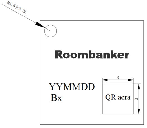
| Code | Bx | YY | MM | DD |
|---|---|---|---|---|
| Explanation | Production batch | Year | Month | Day |
| Code - printing | B1 | 24 | 06 | 27 |
Mark accuracy:20um~40um
Mark depth:±50um
2.3 Pin Definition

| Pin number | symbol | IO type | function |
|---|---|---|---|
| 1 | GND | P | Chip power reference ground |
| 2 | VCC | P | Power supply pins of the chip (typical supply voltage: 3.3V) |
| 3 | PD3 | I/O | general I/O (Configurable features) |
| 4 | PD2 | I/O | general I/O (Configurable features) |
| 5 | GND | P | Chip power reference ground |
| 6 | GND | P | Chip power reference ground |
| 7 | PC0 | I/O | general I/O (Configurable features) |
| 8 | PC1 | I/O | general I/O (Configurable features) |
| 9 | PC2 | I/O | general I/O (Configurable features) |
| 10 | PC3 | I/O | general I/O (Configurable features) |
| 11 | PC4 | I/O | general I/O (Configurable features) |
| 12 | PC5 | I/O | general I/O (Configurable features) |
| 13 | PC6 | I/O | general I/O (Configurable features) |
| 14 | PC7 | I/O | general I/O (Configurable features) |
| 15 | RST | I | Chip hardware reset pin, default high level, effective when pulled low |
| 16 | PB0 | I/O | general I/O (Configurable features) |
| 17 | PB1 | I/O | general I/O (Configurable features) |
| 18 | GND | P | Chip power reference ground |
| 19 | ANT | I/O | RF transmitting and receiving pi |
| 20 | PA0 | I/O | general I/O (Configurable features) |
| 21 | PA1 | I/O | general I/O (Configurable features) |
| 22 | PA2 | I/O | general I/O (Configurable features) |
| 23 | PA3 | I/O | general I/O (Configurable features) |
| 24 | PA4 | I/O | general I/O (Configurable features) |
| 25 | PA5 | I/O | general I/O (Configurable features) |
| 26 | PA6 | I/O | general I/O (Configurable features) |
| 27 | PA7 | I/O | general I/O (Configurable features) |
| 28 | PA8 | I/O | general I/O (Configurable features) |
| GPIO | Alternate Functions |
|---|---|
| PA00 | IADC0.VREFP |
| PA01 | GPIO.SWCLK |
| PA02 | GPIO.SWDIO |
| PA03 | GPIO.SWV,GPIO.TDO,GPIO.TRACEDATA0,LESENSE.EN_0 |
| PA04 | GPIO.TDI,GPIO.TRACECLK,LESENSE.EN_1 |
| PA05 | GPIO.TRACEDATA1,GPIO.EM4WU0,LESENSE.EN_2 |
| PA06 | GPIO.TRACEDATA2 |
| PA07 | GPIO.TRACEDATA3 |
| PB00 | VDAC0.CH0_MAIN_OUT |
| PB01 | GPIO.EM4WU3,VDAC0.CH1_MAIN_OUT |
| GPIO | Alternate Functions |
| PC0 | GPIO.EM4WU6 |
| PC05 | GPIO.EM4WU7 |
| PC0 | GPIO.EM4WU8,GPIO.THMSW_EN |
| PD02 | GPIO.EM4WU9 |
2.4 Topology & Usage

3. Specification
3.1 Technical Specification
| Model | RB4331 | RB8681 | RB9151 |
|---|---|---|---|
| Frequency Band | 433.12MHz~435.12MHz | 863 MHz ~ 870 MHz | 902 MHz ~ 928 MHz |
| Antenna Option | U.FL, RF pad | U.FL, RF pad | U.FL, RF pad |
| RAM | 64 KB | 64 KB | 64 KB |
| Flash | 512 KB | 512 KB | 512 KB |
| RF Data Rate | 2 kbps ~ 100 kbps | 2 kbps ~ 100 kbps | 2 kbps ~ 100 kbps |
| Transmit Range | Up to 3.5 km(Open Area) | Up to 3.5 km(Open Area) | Up to 3.5 km(Open Area) |
| Transmit Power | Max. 20dBm | Max. 20dBm | Max. 20dBm |
| Receiver ensitivity | -110.7 dBm @50kbps(2GFSK) | -113.3 dBm @38.4kbps(2GFSK) | -96.9 dBm @2Mbps(2GFSK) |
| Modulation | FSK / DSSS | FSK / DSSS | FSK / DSSS |
| Digital I/O | 21-ch Digital I/O | 21-ch Digital I/O | 21-ch Digital I/O |
| Analog Input | 21-ch Analog Inputs | 21-ch Analog Inputs | 21-ch Analog Inputs |
| Networking Topology | Star | Star | Star |
| Encryption | AES-CCM+Random Number Key | AES-CCM+Random Number Key | AES-CCM+Random Number Key |
| Image Transmit | Support | Support | Support |
| OTA | Support | Support | Support |
| Supply Voltage | 1.7 V ~ 3.8V | 1.7 V ~ 3.8V | 1.7 V ~ 3.8V |
| Transmit Current | Max 76.8 mA(20dBm) | Max 90.6 mA(20dBm) | Max 92 mA(20dBm) |
| Receive Current | 6.7@ (2-GFSK, 100kbps) | 6.3@ (2-GFSK, 38.4kbps) | 8.5@ (2-GFSK, 2 Mbps) |
| Sleep Current | < 2 μA | < 2 μA | < 2 μA |
| Dimension | 10mm × 10mm × 1.72mm | 10mm × 10mm × 1.72mm | 10mm × 10mm × 1.72mm |
| Weight | 1.8g | 1.8g | 1.8g |
| Operating Temperature | -40 °C ~ 85 °C | -40 °C ~ 85 °C | -40 °C ~ 85 °C |
| Storage Temperature | -40℃ ~ 125℃ | -40℃ ~ 125℃ | -40℃ ~ 125℃ |
| ETSI (Europe) | CE/RED | CE/RED | CE/RED |
| RoHS | Compliant | Compliant | Compliant |
3.2 Absolute Maximum Ratings
| Parameter | Test Condition | Min | Max | Unit |
|---|---|---|---|---|
| Storage temperature range | -50 | +150 | °C | |
| Voltage on any supply pin | -0.3 | 3.8 | V | |
| Total current into VDD power lines | Source | - | 200 | mA |
| Total current into VSS ground lines | Sink | - | 200 | mA |
| Current per I/O pin | Sink | - | 50 | mA |
| Current per I/O pin | Source | - | 50 | mA |
| Current for all I/O pins | Sink | - | 200 | mA |
| Current for all I/O pins | Source | - | 200 | mA |
3.3 General Operating Conditions
| Parameter | Min | Typ | Max | Unit |
|---|---|---|---|---|
| Operating ambient tempera ture range | -40 | - | +85 | °C |
| VDD supply Voltage | 1.71 | 3.3 | 3.8 | V |
| IOVDD operating supply voltage | 1.71 | 3.3 | 3.8 | V |
3.4 Power Consumption
| Parameter | Test Condition | Min | Typ | Max | Unit |
|---|---|---|---|---|---|
| Receive mode | f = 915 MHz, 2-GFSK, 2 Mbps | - | 8.5 | - | mA |
| Receive mode | f = 868 MHz, 2-GFSK, 38.4 kbps | - | 6.3 | - | mA |
| Receive mode | f = 433 MHz, 2-GFSK, 100 kbps | - | 6.7 | - | mA |
| Transmit mode ,EM1 | f = 915 MHz, CW, 20 dBm PA, +20 dBm output power | - | 92 | - | mA |
| Transmit mode ,EM1 | f = 869.5 MHz, CW, 20 dBm PA, +20 dBm output power | - | 90.6 | - | mA |
| Transmit mode ,EM1 | f = 433 MHz, CW, 20 dBm PA, +20 dBm output power | - | 76.8 | - | mA |
| Retained RAM bank in EM2 or EM3. | - | 0.1 | - | µA |
3.5 Clock Sources
Internal High Frequency Clock for RF Stability: 39 MHz Crystal Frequency Tolerance.
| Parameters | Test Condition | Min | Typ | Max | Unit |
|---|---|---|---|---|---|
| Crystal frequency | 39 | MHz | |||
| Equivalent Series Resistance | - | - | 30 | Ω | |
| Load Capacitance | 12 | pF | |||
| Shunt Capacitance | - | - | 3 | pF | |
| Frequency Tolerance | At 25℃±3℃ | -8 | - | 8 | |
| Frequency Stability | Over Operating Temp.Range(Ref.to 25℃) | -10 | - | 10 | ppm |
Internal Low Frequency Clock for BLE Synchronization: 32.768 kHz Crystal Frequency Tolerance.
| Parameters | Test Condition | Min | Typ | Max | Unit |
|---|---|---|---|---|---|
| Crystal frequency | 32.768000 | KHz | |||
| Equivalent Series Resistance | - | 80 | KΩ | ||
| Load Capacitance | 12.5 | pF | |||
| Shunt Capacitance | - | 1.15 | - | pF | |
| Frequency Tolerance | At 25℃±3℃ | -10 | - | 10 |
4. QA Requirement
| Information Description | Standard(Yes) Custom(No) |
|---|---|
| ESD Testing | Yes |
| RF Antenna Analysis | Yes |
| Environmental Testing | Yes |
| Reliability Testing | Yes |
| Certification | FCC,CE, RoHS |
5. Sub-GHz RF Transceiver Characteristics
5.1 915 MHz Band +20 dBm RF Characteristics
Conditions: 25ºC, VCC=3.3V, RF center frequency 915 MHz.
| Parameter | Test Condition | Min | Typ | Max | Unit |
|---|---|---|---|---|---|
| RF test frequency range | 902 | - | 928 | MHz | |
| Maximum TX Power | PAVDD = 3.3V, 20 dBm devices, +20 dBm match | 17.7 | 20 | 21.4 | dBm |
| Minimum active TX Powe | - | -20.6 | - | dBm | |
| Max usable input level, 0.1% BER | Desired is reference 2 Mbps 2GFSK signal | - | - | 10 | dBm |
| Sensitivity | |||||
| Desired is reference 4.8 kbps OOK signal, PER<20% | - | -113.1 | - | dBm | |
| Desired is reference 50 kbps 2FSK signal, Δf = ± 25 kHz, PER<10% | - | -110.1 | - | dBm | |
| Desired is reference 50 kbps 2FSK signal, Δf = ± 25 kHz, PER | - | -114.2 | - | dBm | |
| Desired is reference 150 kbps 2FSK signal, Δf = ± 37.5 kHz, PER<10% | - | -107.5 | - | dBm | |
| Desired is reference 2 Mbps 2GFSK signal, Δf = ± 500 kHz, BER<0.1% | - | -96.9 | - | dBm | |
| Desired is reference 4.8 kbps O QPSK signal, spreading factor=8, PER<1% | - | -125.8 | - | dBm | |
| Desired is reference 250 kbps O QPSK DSSS signal, PER<1% | - | -103.5 | - | dBm | |
| Desired is reference 120 kbps OOK signal8, PER<20% | - | -102.6 | - | dBm |
5.2 868 MHz Band +20 dBm RF Characteristics
Conditions: 25ºC, VCC=3.3V, RF center frequency 868 MHz.
| Parameter | Test Condition | Min | Typ | Max | Unit |
|---|---|---|---|---|---|
| RF test frequency range | 868 | 869.9 | MHz | ||
| Maximum TX Power | PAVDD = 3.3V, 20 dBm devices, +20 dBm match | 18.4 | 20.3 | 21.5 | dBm |
| Minimum active TX Powe | - | -20.4 | - | dBm | |
| Max usable input level, 0.1% BER | Desired is reference 500 kbps 2GMSK signal | - | - | 10 | dBm |
| Sensitivity | |||||
| Desired is reference 2.4 kbps 2GFSK signal, Δf = ± 1.2 kHz, BER<0.1% | - | -125.3 | - | dBm | |
| Desired is reference 38.4 kbps 2GFSK signal, Δf = ± 20 kHz, BER<0.1% | - | -113.3 | - | dBm | |
| Desired is reference 50 kbps 2FSK signal, Δf = ± 12.5 kHz, PER<10% | - | -111.5 | - | dBm | |
| Desired is reference 100 kbps 2FSK signal, Δf = ± 25 kHz, PER<10% | - | -109.2 | - | dBm | |
| Desired is reference 500 kbps 2GMSK signal, Δf = ± 125 kHz1, BER<0.1% | - | -103.2 | - | dBm | |
| Desired is reference 100 kbps O QPSK DSSS signal, PER<1% | - | --110.9 | - | dBm |
5.3 433 MHz Band +20 dBm RF Characteristics
Conditions: 25ºC, VCC=3.3V, RF center frequency 433 MHz.
| Parameter | Test Condition | Min | Typ | Max | Unit |
|---|---|---|---|---|---|
| RF test frequency range | 433.12 | 434.72 | MHz | ||
| Maximum TX Power | PAVDD = 3.3V, 20 dBm devices, +20 dBm match | 17.6 | 19.8 | 21.1 | dBm |
| Minimum active TX Powe | - | -20.3 | - | dBm | |
| Max usable input level, 0.1% BER | Desired is reference 100 kbps 2GFSK signal, BER<0.1%l | - | - | 10 | dBm |
| Sensitivity | |||||
| Desired is reference 2.4 kbps 2GFSK signal, Δf = ± 1.2 kHz, BER<0.1% | - | -126.9 | - | dBm | |
| Desired is reference 4.8 kbps OOK signal, PER<20% | - | -114.2 | - | dBm | |
| Desired is reference 100 kbps 2GFSK signal, Δf = ± 50 kHz, BER<0.1% | - | -110.7 | - | dBm | |
| Desired is reference 50 kbps 2GFSK signal, Δf = ± 25 kHz, BER<0.1% | - | -113.8 | - | dBm | |
| Desired is reference 50 kbps 4GFSK signal, Δfo = ± 25 kHz, Δfi = ± 8.33 kHz, PER<1% | - | -112.1 | - | dBm | |
| Desired is reference 460 MHz 4.8 kbps 2FSK signal, Δf = ± 2.4 kHz, PER<10% | - | -122.5 | - | dBm |
6. Hardware Design Considerations
- The RBF chips of model 915/868/433 MHz have built-in RF chip matching circuits, eliminating the need for external placement of chip matching devices and saving board space.
- The RBF chips of model 15/868/433MHZ have all integrated peripheral chips such as 39M crystal oscillator and 32.768K crystal oscillator.
- The chip should not be placed in a casing made of metal. If a metal casing must be used, the antenna must be led out.
- For the products that require installation of this chip, some metal components such as screws and inductors should be kept as far away as possible from the RF antenna part of the chip.
- On the antenna of the chip, try not to place other components to avoid interference with the wireless performance.
- The chip should be placed as close as possible to the edge or corner of the main board, and the PCB under the antenna part of the chip should be annotated and hollowed out with the keep out layer if it is not possible to hollow out. If copper plating or wiring is not allowed under the antenna, it will affect the RF performance.
- Please pay attention to check the pin diagrams and the IO connected to them. Please pay attention to the IO mode and status.
- GND must be well grounded.
- It is recommended to use magnetic beads or inductors for filtering of the input power supply.
7. Antenna layout suggestion
For RBF series chips, the internal integrated chip matching, customers only need to build an antenna matching circuit based on the external antenna.
For RBF series chip antenna design, it is recommended to reserve antenna matching devices. Because the RBF series chip frequency is 433MHz/868MHz/915MHz, the onboard antenna size is too large, it is not recommended to use the onboard antenna.
When using IPEX technology (external antenna), it is necessary to pay attention to the need for 50 Ohm matching in the RF output part, and it is recommended to cover the RF output part in the PCB layout by connecting holes to the ground to prevent unnecessary losses during the transmission of RF on the PCB board. And the RF part needs to be kept at a distance of more than 10mm from some interference sources, and the general layout needs to avoid any electrical components.

8. Package Information
| Parameter | Value |
|---|---|
| Packing Type | Tape Reel |
| Packing Quantity | 100 pcs/ tape |